
0x5A — The Command That Lets Flash Chips Describe Themselves

SPI NOR flash has been a boot firmware workhorse for decades. But for most of that history, every flash chip was a black box — you either had the datasheet hardcoded into your bootloader, or you were in trouble.
JEDEC fixed this with JESD216: the Serial Flash Discoverable Parameters (SFDP) standard. And the key that unlocks it all is a single command byte: 0x5A.
The Problem: Every Flash Chip Was a Snowflake
Before SFDP, firmware had to maintain a lookup table mapping JEDEC manufacturer IDs to flash capabilities. See ID 0xC2 (Macronix)? Great, now check the model byte. Model 0x20? That’s 3V, 256Mb, Quad I/O. Model 0x19? Different erase sizes, slower max frequency.
This broke in three ways:
New chips broke old firmware — a new density variant with the same ID bytes needed a code update.
Dead chips killed boot — if your lookup table was in flash and your flash died, you couldn’t discover a replacement.
Every vendor had their own quirks — same density, same I/O, different erase granularity. Your table grew endlessly.
The industry needed the flash chip to declare its own capabilities — not rely on the host to already know them.
Enter SFDP: Flash Self-Description
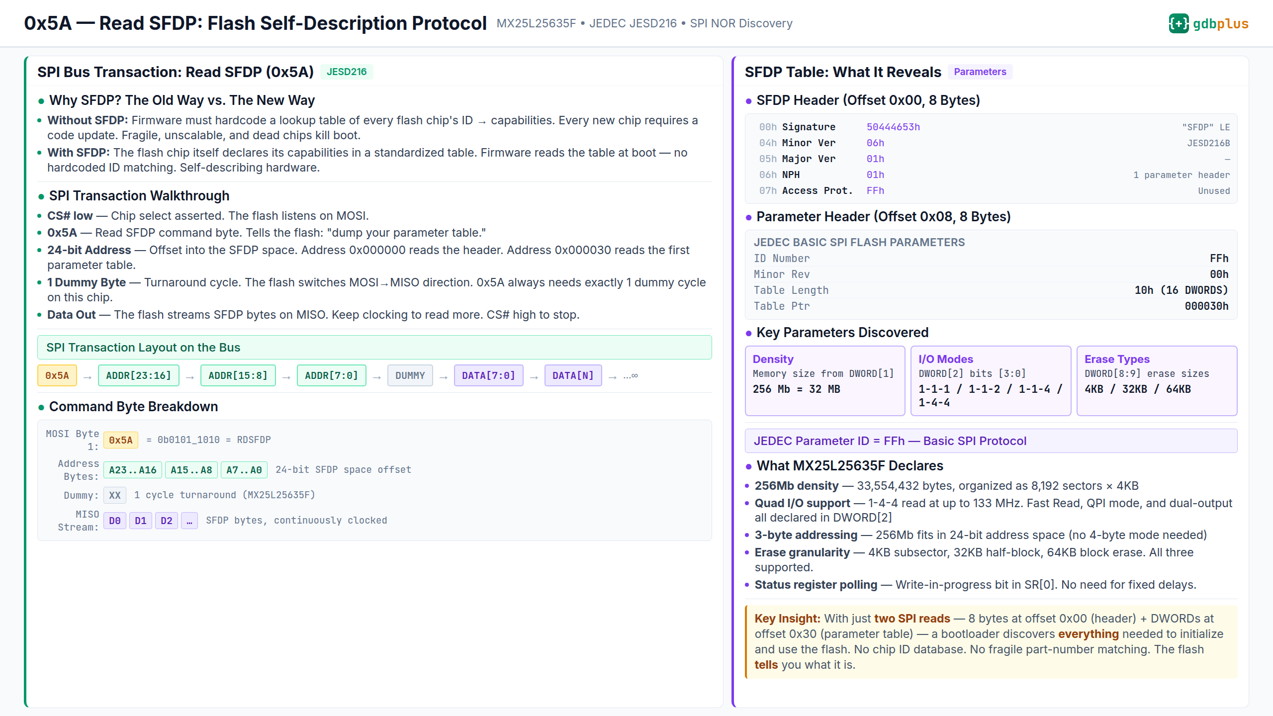
JEDEC JESD216 defines the SFDP standard. Every compliant flash chip stores a structured parameter table in a dedicated internal ROM area. The host reads this table at boot using command 0x5A (Read SFDP, or RDSFDP).
The transaction is straightforward:
▸ CS# low — Assert chip select. The flash is now listening.
▸ 0x5A — Send the RDSFDP command byte on MOSI. This is the magic number.
▸ 24-bit Address — 3 bytes specifying the offset into the SFDP address space. The SFDP table lives in its own memory map, separate from the main flash array. Address 0x000000 reads the SFDP header.
▸ 1 Dummy Byte — One turnaround cycle. The flash switches its internal data path from MOSI (receiving) to MISO (transmitting). On the MX25L25635F, 0x5A always needs exactly 1 dummy cycle — this is declared in the SFDP table itself.
▸ Continuous Clock — Keep toggling SCK. The flash streams SFDP data bytes on MISO until you stop. Pull CS# high to end the transaction.
The SFDP Header: 8 Bytes That Unlock Everything
Reading offset 0x00 returns the 8-byte SFDP header:
From JESD216 Section 6.3:
▸ Signature (Bytes 0–3): 0x50444653. That’s “SFDP” in ASCII, stored little-endian (”S” = 0x53 is byte 0, “P” = 0x50 is byte 1...). If these 4 bytes don’t match, the flash doesn’t support SFDP — fall back to the old ID lookup.
▸ Minor Version (Byte 4): 0x06 on the MX25L25635F. This maps to JESD216B, which added support for 4-byte addressing and additional parameter tables.
▸ Major Version (Byte 5): 0x01. Combined with minor, this tells you which version of the JESD216 spec the table follows.
▸ NPH — Number of Parameter Headers (Byte 6): 0x01 on the MX25L25635F. This chip has one parameter table. High-end flash might have 2–3 (basic SPI + 4-byte addressing + sector map).
▸ Access Protocol (Byte 7): 0xFF. Reserved/unused for standard SPI flash.
The Parameter Header: Where to Go Next
Immediately after the SFDP header (offset 0x08), the parameter header tells you where the actual capability data lives:
From JESD216, each parameter header is 2 DWORDs (8 bytes):
▸ Parameter ID (Byte 0): 0xFF. This is the JEDEC-assigned ID for the “Basic SPI Flash Parameters” table — the one every SPI NOR flash must provide.
▸ Minor Revision (Byte 1): 0x00. Version of this specific parameter table.
▸ Table Length (Byte 2): Number of DWORDs in the table. For basic SPI, typically 16 DWORDs (0x10).
▸ Table Pointer (Bytes 4–6): 3-byte address where this parameter table starts in the SFDP space. On the MX25L25635F, this is 0x000030.
With the pointer in hand, you issue a second 0x5A command — this time with address 0x000030 — and read the 16-DWORD parameter table.
What the Parameter Table Reveals About MX25L25635F
The 16 DWORDs (64 bytes) of the basic SPI parameter table tell you everything:
▸ DWORD[1] — Flash Density: The first DWORD after the parameter header encodes the total memory size as a bit count. For 256 megabits, this field returns 0x1FFFFFFF or similar encoding, allowing the host to compute 2^N bytes. The MX25L25635F reports 256Mb = 32MB = 33,554,432 bytes.
▸ DWORD[2] — I/O Mode Support: Bits [3:0] declare the supported read commands. The MX25L25635F advertises four modes — 1-1-1 (standard SPI, 0x03), 1-1-2 (dual output, 0x3B), 1-1-4 (quad output, 0x6B), and 1-4-4 (quad I/O, 0xEB). This lets the bootloader auto-select the fastest read mode the flash supports.
▸ DWORD[2] — Maximum Frequency: Bit [30] indicates support for >100MHz. The MX25L25635F supports up to 133MHz in quad I/O read mode.
▸ DWORD[4] — Erase Types: Three erase instruction sizes are declared. Type 1 = 4KB subsector erase (0x20), Type 2 = 32KB half-block erase (0x52), Type 3 = 64KB block erase (0xD8). The flash advertises typical erase times for each type, so the host can set appropriate timeouts without guessing.
▸ DWORD[7] — Status Register Polling: Bit [3] declares whether the flash supports software write-in-progress polling via the status register. The MX25L25635F sets this bit, meaning the host can poll SR[0] instead of using fixed delays after each write/erase. This is critical for fast flash update performance.
▸ DWORD[9–10] — 4-Byte Addressing: Since 256Mb fits in a 24-bit address space (2^24 × 8 bits = 128Mb, but 256Mb = 2^28 bits, and with page/block organization, addressing is byte-based: 32MB = 2^25 bytes), the MX25L25635F uses 3-byte addressing natively. Bits in DWORD[9] confirm this — no 4-byte address mode is needed.
▸ DWORD[15] — Quad Enable Requirements: Declares whether QE (Quad Enable) sits in a non-volatile status register (requiring Write Status Register to toggle) or a volatile configuration register. The MX25L25635F uses SR[6] as the QE bit — non-volatile, so it survives power cycles but needs explicit clearing if you want to run in 1-1-1 mode.
Why This Matters in UEFI / EDK2 Firmware
In the EDK2 firmware stack, SPI NOR flash initialization typically happens inside a platform-specific PEIM (Pre-EFI Initialization Module) or early DXE driver. The conventional approach uses the JEDEC ID (command 0x9F) to look up flash parameters from a hardcoded table.
SFDP changes the flow:
▸ Read 0x9F (JEDEC ID) — Get manufacturer and model bytes. This still runs first, because 0x9F works on every SPI flash ever made. But now it’s just for logging and sanity checks.
▸ Read 0x5A (SFDP Header at offset 0x00) — Verify the “SFDP” signature (0x50444653). If it’s there, proceed with SFDP. If not, fall back to the legacy lookup.
▸ Read 0x5A (Parameter Table at pointer offset) — Parse the 16-DWORD basic SPI parameter table. Extract density, supported I/O modes, erase types, timing parameters, and status register layout.
▸ Auto-configure the SPI protocol — Based on DWORD[2], select the fastest supported read command (1-4-4 if available, 1-1-4 as minimum quad). Based on DWORD[4], configure the flash block driver with the correct erase opcodes and timeout values.
▸ Validate with 0x9F — Confirm the manufacturer ID matches and that the model is consistent with the SFDP declarations. Log any discrepancies.
This eliminates the fragile ID→capability lookup table entirely. New Macronix, Winbond, or GigaDevice chips drop in with no firmware change. The flash tells you what it can do.
SPI Bus Details: Why One Dummy Byte?
The dummy byte in the 0x5A transaction isn’t arbitrary — it’s the turnaround cycle where the SPI bus changes direction. On a standard SPI bus, the master controls MOSI (Master Out, Slave In) while the slave drives MISO (Master In, Slave Out).
When you send 0x5A + 3 address bytes, the flash is listening on MOSI. After the address, it needs time to:
Decode the SFDP offset address
Switch its internal data path from receiving to transmitting
Start clocking out the first SFDP data byte on MISO
The dummy byte buys this time. On slower SPI modes (single I/O), one cycle is enough. In quad I/O read mode (command 0xEB), some chips need 4–8 dummy cycles because the quad data path takes longer to set up.
The SFDP table itself tells you how many dummy cycles each command needs — DWORD[2] bits [7:5] specify the mode bits and dummy cycle count for the Read SFDP command specifically. This is self-referential: the parameter table declares how to read the parameter table.
Beyond Basic SPI: SFDP’s Extensible Design
JESD216 isn’t limited to basic SPI parameters. Additional parameter tables cover:
▸ 4-Byte Addressing (Parameter ID 0x84): For flash chips >256Mb that need 32-bit addresses. The table declares which commands support 4-byte addressing mode and how to toggle it.
▸ Sector Map (Parameter ID 0x81): For chips with uniform or hybrid sector layouts. Declares the erase granularity for each address region. Essential for flash file systems that need to know block boundaries.
▸ OTP / Security Registers (Parameter ID 0x8C): One-time programmable regions, serial numbers, and lock bits. The SFDP table declares their location, size, and access protocol.
The MX25L25635F exposes only the basic SPI parameter table (ID 0xFF), but higher-end Macronix chips add 4-byte addressing and sector map tables. The SFDP header’s NPH field tells you how many to expect — just iterate through them.
Real-World Adoption
SFDP is now mandatory for any flash chip targeting modern platforms:
▸ Intel PCH SPI programming guide recommends SFDP-based discovery for all attached SPI NOR flash since Skylake generation (2015+).
▸ Linux kernel’s spi-nor subsystem has been SFDP-first since kernel 4.x. The spi_nor_scan() function in drivers/mtd/spi-nor/core.c reads SFDP before falling back to the legacy ID table.
▸ U-Boot bootloader uses SFDP in its spi-flash framework. The spi_flash_scan() logic reads the SFDP header and parameter tables during the flash probe sequence.
▸ Coreboot calls SFDP “the right way” and strongly discourages new ID-table entries for chips that support SFDP correctly.
The Bottom Line
0x5A is a simple command — one byte, three address bytes, one dummy byte, infinite data out. But it represents a fundamental shift in how firmware interacts with hardware: from “I know what you are” to “tell me what you are.“
For the MX25L25635F, two 0x5A reads replace a 100-entry manufacturer ID lookup table. For the firmware engineer, it means never having to add “just one more flash chip” to the bootloader again.
The flash chip that describes itself is the flash chip that survives firmware updates, silicon revisions, and supply-chain substitutions. 0x5A is how you ask.
#sfdp #spi #norflash #firmware #embedded #macronix #mx25l25635f #jedec #bootloader #uefi #gdbplus